['electroncircuits.blogspot.com'];
Showing posts with label Chargers Projects. Show all posts

How to Power Your USB Gadgets with Bike


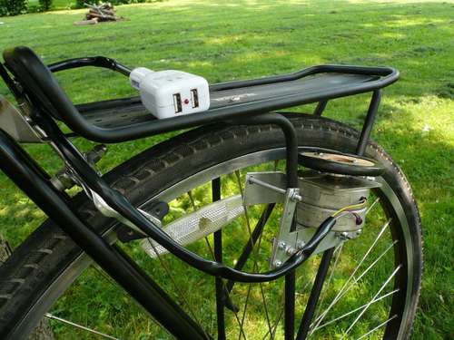
Power USB Gadgets With Your Bike
With more and more gadgets coming out every day that utilize USB for charging, it’s almost necessary to have a USB port available at all times.  This DIYer decided to create a 5V generator using his bike and a modified USB car charger. The 5V USB plugs are situated under his seat and he has a carrying rack for cellphones, GPS, or MP3 players on the go.
Power USB Gadgets With Your Bike
The USB bike generator works by placing a rotating wheel perpendicular to the rear wheel of the bike with a heavy spring. The mini-wheel turns a stepper motor to generate a charge that is then smoothed out by an in-line rectifier.[Link]

Solar Lamp using the PR4403

The PR4403 is an enhanced cousin of the PR4402 40 mA LED driver. It has an extra input called LS which can be taken low to  turn the LED on. This makes it very easy  to build an automatic LED lamp using a  rechargeable battery and a solar module. The LS input is connected directly to the solar cell, which allows the module to be  used as a light sensor at the same time as  it charges the battery via a diode. When  darkness falls so does the voltage across  the solar module: when it is below a thresh-old value the PR4403 switches on. During  the day the battery is charged and, with  the LED off, the driver only draws 100 µA.
Circuit Diagram :
Solar Lamp-Circuit Diagram
At night the energy stored in the battery is released into the LED. In contrast to similar designs, here we can make do with a single  1.2 V cell. The PR4403 is available in an SO-8 pack-age with a lead pitch of 1.27 mm. The  other components are a 1N4148 diode (or a Schottky 1N5819) and a 4.7 µH choke. Pin 2 is the LS enable input, connected directly to the solar module. According to the datasheet, it is possible to connect a series resistor at this point (typ. 1.2 M) to increase the effective threshold voltage. The LED will then turn on slightly earlier in the evening before it is not completely  dark. Pins 3 and 6 of the device must be connected together and together form the output of the circuit.
Author : Burkhard Kainka - Copyright : Elektor

A 12V Car Charger For ASUS Eee Notebook

The ASUS Eee is a fantastic ultra-portable notebook with almost everything required for geeks (and nothing that isn’t). Plus it features fantastic build quality and is very well priced. If you live in New Zealand you can get them from DSE; at the time of writing they are the exclusive supplier. I worked out it’s the same cost as importing one once you include all the duties and tax, plus you get the advantage of a proper NZ-style mains charger. Anyway, being so small I thought it would be nice to be able to carry this around in the car. Unfortunately I couldn’t find a car charger available anywhere at the time so I decided to tackle the problem myself. As a bonus this provides an opportunity for an external high-capacity battery.
asus eee 701
Commercial Equivalent:
I thought at this stage it would be worth noting that a commercial car charger is now available for less than it cost me to build this from Expansys and is available in most countries (select your location on their site). It outputs 9.5v from 10-18v in at up to 2.5A. I’d actually recommend it over the design here is it seems to perform better at lower voltages (that one works down to 10V). However I have kept this page up as a reference for those who enjoy tinkering.
Design:
The charger included with the Eee is rated at 9.5v, 2.315A. There isn’t a fixed voltage regulator available for this exact voltage, so the circuit needed to be designed around an adjustable regulator. I decided to design the charger around the LM2576 “Simple Switcher” IC from National Semiconductor. There are tons of ICs like this available, many of which are a bit more efficient, however I selected this one because it is readily available and relatively cheap. It also has a lower drop-out voltage (~2V) than many other chips I looked at which is important when powering the device from a car or 12v SLA battery.
eee_car_charger_circuit d
This circuit could have used a standard three pin regulator IC such as the LM317, however most types require an external transistor when handling so much current and not to mention the fact that they are very inefficient; they draw the same amount of current from the input as the load and the difference in power is dissipated as heat. The main problem with using the LM2576 is the fact it needs quite a large inductor due to its somewhat low switching frequency. The inductor I used is made by Pulse Engineering, part number PE92108KNL. I’d prefer a smaller one, however I couldn’t find one capable of supplying the required current that I could purchase in single units. Besides the PE92108KNL is apparently designed specifically to work with the LM257x series.
charger_case_opens
The circuit also includes a low voltage cut-out based on a 9.1v Zener diode and BC337 transistor that will shut down the regulator if the input voltage is below 11.5V. This prevents unstable operation of the regulator at lower input voltages, and also helps prevent accidental flattening of the supply battery. Substituting this transistor for similar type may affect the cut-out voltage; the Vbe of the transistor should be 1.2v.All of the components used should be pretty readily available in most areas. I got everything from Farnell. Jaycar also sells everything except the inductor. Make sure you specify high temperature, low ESR capacitors as these help result in more stable operation and better efficiency of the charger.
eee_car_charger_schematic_monow
Unfortunately the end result is a charger that is slightly bulkier than I would really like. I attempted to fit this inside an old mobile phone charger case so the whole thing could hang out of the cigarette lighter, however I ran into trouble making the circuit stable enough and dissipating all the heat. Due to the high current involved compared to a mobile phone charger the components are much bulkier so it’s pretty tricky to get all to fit! If I do get it finished I’ll add an update.
Parts List:
  • 2x 10k resistor (R1 & R4)
  • 2x 22k resistor (R2 & R3)
  • 1x 1.5k resistor (R5)
  • 1x 120μF 25v electrolytic capacitor (C1)
  • 1x 2200μF 16v electrolytic capacitor (C2)
  • 1x 1N5822 Schottky diode (or equivalent)
  • 1x 9.1v 0.5W Zener diode
  • 1x BC337 NPN transistor
  • 1x LM2576T-ADJ IC
  • 1x 100uH, 3A inductor (e.g. Pulse PE92108KNL)
  • 25°C/W or better minature heatsink (e.g. Thermalloy 6073)
  • Cigarette lighter plug with 3A fuse and 2.1mm DC plug (e.g. DSE P1692)
  • 2.1mm DC chassis mount socket
  • 1.7mm x 4.75mm (ID x OD) DC plug and cable
  • Small plastic enclosure
Building It:
Make yourself a PCB using the template below (600dpi). I simply laser print (or photocopy) the design onto OHP transparency sheet and then transfer the toner onto a blank PCB using a standard clothes iron. Any missing spots can be touched up with a permanent marker before etching. This is quick, usually results in pretty tidy boards and hardly costs a thing. There is a tutorial on a variation of this method at http://max8888.orcon.net.nz/pcbs.htm.
eee_car_charger_pcbs
Install the components on the PCB and triple check the layout before soldering. It is much easier to start with the low profile components such as resistors and diodes, then install the larger components after-wards. Don’t forget the wire link; this is shows as a red line on the layout guide above. Remember to smear a small amount of heatsink compound on the regulator tab before mounting the heatsink.
eee_car_charger_pcb_layoute
For a case I used a small plastic enclosure from DSE, part H2840, as it was all the local store had in stock that was remotely suitable. The PCB is designed to fit into this particular case, however any small box should be suitable. If you have a dead laptop charger lying about it might be worth ripping the guts out of that and salvaging the case. If your enclosure is different you may need to modify the design to suit, so I have provided the schematic and PCB design files for download. They were created using Eagle. The Eee uses a standard 1.7mm DC power connector with a positive tip.
eee_car_chargerw1
Testing:
Connect the circuit to a 12v supply. If you use a car or lead acid battery ensure you have a 3A fuse fitted in line with the circuit before connecting it, just in case. Use your multimeter to check that the circuit outputs about 9.45v with no load. Connect a 12V, 21W lamp (e.g. old brake lamp from a car) or similar load across the output and check that the voltage doesn’t vary much. You should now be able to connect your Eee. The circuit design should be good for up to 2.5A, so there is plenty of margin for the Eee to fully function and charge its own battery off this supply.
     eee_external_battery0
SLA Battery Carry-bag:
Jaycar have a really cool carry bag with a shoulder strap designed to perfectly fit a 12v 7AH sealed lead acid battery. The bag features a fused cigarette lighter socket and is the perfect compliment to this charger. It works well with the Eee and provides hours of extra use. The shoulder strap means it’s not too bothersome to carry about and the charger circuit itself zips up neatly inside the bag. The under-voltage cut-off means the battery will never run completely flat, and the Eee will simply cut over to its internal battery once the SLA runs out. I got my SLA battery from Rexel as they are much cheaper (approx NZ$18 including GST last time I bought one) and they don’t sit as long on the shelf as many other suppliers.
inside_bag-charger l
Disclaimer:
This circuit is intended for people who have had experience in constructing electronic projects before. The circuit design and build process are provided simply as a reference for other people to use and I take no responsibility for how they are used. If you proceed with building and/or using this design you do so entirely at your own risk. You are free to use the content on this page as you wish, however I do ask that you include a link or reference back to this page if you distribute or publish any of the content to others.


Deluxe Charge Rate Limiter for Small Capacity NiCad Batteries

Here is a deluxe version of the simple charge rate limiter, using the same idea but with the ability to charge two packs simultaneously from a single wall charger. For circuit description and parts list, see the simple charger page. Since wall chargers provide about 55mA, you should not use this dual circuit to charge batteries at rates greater than 27mA (for a total of 54mA).
charg01    
fancharg02
chrgall03
charg04
charg05

Mobile Cellphone Battery Charger

Charging of the cellphone battery is a big problem while travelling as power supply source is not generally accessible. If you keep your cellphone switched on continuously, its battery will go flat within five to six hours, making the cellphone useless. A fully charged battery becomes necessary especially when your distance from the nearest relay station increases. Here’s a simple charger that replenishes the cellphone battery within two to three hours. Basically, the charger is a current-limited voltage source. Generally, cellphone battery packs require 3.6-6V DC and 180-200mA current for charging. These usually contain three NiCd cells, each having 1.2V rating. Current of 100mA is sufficient for charging the cellphone battery at a slow rate. A 12V battery containing eight pen cells gives sufficient current (1.8A) to charge the battery connected across the output terminals.
Circuit Diagram :
Mobile Cellphone Battery Charger Circuit diagram

The circuit also monitors the voltage level of the battery. It automatically cuts off the charging process when its output terminal voltage increases above the predetermined voltage level. Timer IC NE555 is used to charge and monitor the voltage level in the battery. Control voltage pin 5 of IC1 is provided with a reference voltage of 5.6V by zener diode ZD1. Threshold pin 6 is supplied with a voltage set by VR1 and trigger pin 2 is supplied with a voltage set by VR2. When the discharged cellphone battery is connected to the circuit, the voltage given to trigger pin 2 of IC1 is below 1/3Vcc and hence the flip-flop in the IC is switched on to take output pin 3 high.
Mobile Cellphone Battery Charger
When the battery is fully charged, the output terminal voltage increases the voltage at pin 2 of IC1 above the trigger point threshold. This switches off the flip-flop and the output goes low to terminate the charging process. Threshold pin 6 of IC1 is referenced at 2/3Vcc set by VR1. Transistor T1 is used to enhance the charging current. Value of R3 is critical in providing the required current for charging. With the given value of 39-ohm the charging current is around 180 mA.
The circuit can be constructed on a small general-purpose PCB. For calibration of cut-off voltage level, use a variable DC power source. Connect the output terminals of the circuit to the variable power supply set at 7V. Adjust VR1 in the middle position and slowly adjust VR2 until LED1 goes off, indicating low output. LED1 should turn on when the voltage of the variable power supply reduces below 5V. Enclose the circuit in a small plastic case and use suitable connector for connecting to the cellphone battery.

Note. At EFY lab, the circuit was tested with a Motorola make cellphone battery rated at 3.6V, 320 mAH. In place of 5.6V zener, a 3.3V zener diode was used. The charging current measured was about 200 mA.The status of LED1 is shown in the table.
Author :  Mohan kumar  Copyright : www.efymag.com

A Simple NiCd Charger Circuit Diagram

A simple NiCd charger can be built using ‘junk box’ components and an inexpensive LM317 or 78xx voltage regulator. Using a current limiter composed of R3 and a transistor, it can charge as many cells as desired until a ‘fully charged’ voltage determined by the voltage regulator is reached, and it indicates whether it is charging or has reached the fully charged state. If the storage capacitor (C1) is omitted, pulsed charging takes place. In this mode, a higher charging current can be used, with all of the control characteristics remaining the same.
The operation of the circuit is quite simple. If the cells are not fully charged, a charging current flows freely from the voltage regulator, although it is limited by resistor R3 and transistor T1. The limit is set by the formula Imax ≈ (0.6 V) ÷ R3 For Imax = 200 mA, this yields R3 = 3 Ω. The LED is on if current limiting is active, which also means that the cells are not yet fully charged. The potential on the reference lead of the voltage regulator is raised by approximately 2.9 V due to the voltage across the LED.
Circuit Diagram :
A Simple Nicd Charger Circuit Diagram
This leads to a requirement for a certain minimum number of cells. For an LM317, the voltage between the reference lead and the output is 1.25 V, which means at least three cells must be charged (3 × 1.45 V > 2.9 V + 1.25 V). For a 78xx with a voltage drop of around 3 V (plus 2.9 V), the minimum number is four cells. When the cells are almost fully charged, the current gradually drops, so the current limiter becomes inactive and the LED goes out.
In this state, the voltage on the reference lead of the regulator depends only on voltage divider R1/R2. For a 7805 regulator, the value of R2 is selected such that the current through it is 6 mA. Together with the current through the regulator (around 4 mA), this yields a current of around 10 mA through R1. If the voltage across R1 is 4 V (9 V – 5 V), this yields a value of 390 Ω. The end-of-charge voltage can thus be set to approximately 8.9 V. As the current through the regulator depends on the device manufacturer and the load, the value of R1 must be adjusted as necessary. The value of the storage capacitor must be matched to the selected charging current. As already mentioned, it can also be omitted for pulse charging.
Author: Wolfgang Schmidt   Copyright: Elektor

Switchless NiCd/NiMH Charger Circuit

This circuit may be used to replace the single current limiting resistor often found in dirt cheap battery chargers. The alternative shown here will eventually pay off because you no longer have to throw away your NiCds after three months or so of maltreatment in the original charger. The circuit diagram shows an LM317 in constant-current configuration but without the usual fixed or variable resistor at the ADJ pin to determine the amount of output current. Also, there is no switch with an array of different resistors to select the charge currents for three cell or battery types we wish to charge: AAA, AA and PP3 (6F22). When, for example, an empty AAA cell is connected, the voltage developed across R1 causes T1 to be biased via voltage dropper D1. This results in about 50 µA flowing from the LM317’s ADJ pin into the cell, activating the circuit into constant-current mode. D4 is included to prevent the battery being discharged when the charger is switched off or without a supply voltage.
Circuit diagram:
switchless nicd nimh charger circuit diagram
The charging current I is determined by R1/R3/R3 as in R(n) = (1.25 + Vsat) / I where Vsat is 0.1 V. The current should be one tenth of the nominal battery capacity — for example, 170 mA for a 1700-mAh NiCd AA cell. It should be noted that ‘PP3’ rechargeable batteries usually contain seven NiCd cells so their nominal voltage is 8.4 V and not 9V as is often thought. If relatively high currents are needed, the power dissipation in R1/R2/R3 becomes an issue. As a rule of thumb, the input voltage required by the charger should be greater than three times the cell or battery (pack) voltage. This is necessary to cover the LM317’s dropout voltage and the voltage across R(n). Two final notes: the LM317 should be fitted with a small heat sink. With electrical safety in mind the use of a general-purpose mains adapter with DC output is preferred over a dedicated mains transformer/rectifier combination.
Author: Myo Min Copyright: Elektor

A Friendly Charger Circuit for Mobile Phones

Most mobile chargers do not have current/voltage regulation or short-circuit protection. These chargers provide raw 6-12V DC for charging the battery pack. Most of the mobile phone battery packs have a rating of 3.6V, 650mAh. For increasing the life of the battery, slow charging at low current is advisable. Six to ten hours of charging at 150-200mA current is a suitable option. This will prevent heating up of the battery and extend its life.

Circuit diagram:

A Friendly Charger Circuit  For Mobile Phones A Friendly Charger Circuit Diagram For Mobile Phones

Parts:

Resistors:
P1 = 10K LOG
R1 = 1K
R2 = 1K
R3 = 1K
R4 = 1K
R5 = 3.3K
R6 = 16R/2W
R7 = 220R
R8 = 3.3R
R9 = 1K

Capacitors:

C1 = 470uF/25V
C2 = 10uF/25V
C3 = 1KuF/25V

Semiconductors:

D1 = Red LED
D2 = Green LED
Q1 = BC547
Q2 = BD677
ZD1 = 12V/1W
ZD2 = 5.6V/1W
IC1 = CA3130

Description:

The circuit described here, provides around 180mA current at 5.6V and protects the mobile phone from unexpected voltage fluctuations that develop on the mains line. So the charger can be left ‘on’ over night to replenish the battery charge. The circuit protects the mobile phone as well as the charger by immediately disconnecting the output when it senses a voltage surge or a short circuit in the battery pack or connector. It can be called a ‘middle man’ between the existing charger and the mobile phone.

It has features like voltage and current regulation, over-current protection, and high- and low-voltage cut-off. An added specialty of the circuit is that it incorporates a short delay of ten seconds to switch on when mains resumes following a power failure. This protects the mobile phone from instant voltage spikes. When short-circuit occurs at the battery terminal, resistor R8 senses the over-current, allowing Q1 to conduct and light up D1. Glowing of D2 indicates the charging mode, while D1 indicates short-circuit or over-current status.

The value of resistor R8 is important to get the desired current level to operate the cut-off. With the given value of R8 (3.3 ohms), it is 350 mA. Charging current can also be changed by increasing or decreasing the value of R7 using the ‘I=V/R’ rule. Construct the circuit on a common PCB and house in a small plastic case. Connect the circuit between the output lines of the charger and the input pins of the mobile phone with correct polarity.

Author : D. Mohan Kumar Copyright : E F Y


Electric Window/Fence Charger

Here is the circuit of a simple electric window charger. With a couple of minor circuit variations, it can be used as an electric fence charger too. A standard 12V, 7Ah sealed maintenance-free (SMF) UPS battery is required for powering the entire unit. Any component layout and mounting plan can be used. However, try to keep the output terminals of transformer X1 away from the circuit board. Timer NE555 (IC1) is wired as a free-running oscillator with narrow negative pulse at the output pin 3. The pulse frequency is determined by resistors R2 and R3, preset VR1 and capacitor C3. The amplitude of the output pulse can be varied to some extent by adjusting variable resistor VR1. You can vary the frequency from 100 Hz to 150 Hz. X1 is a small, iron-core, step-down transformer (230V AC primary to 12V, 1A secondary) that must be reverse connected, i.e., the secondary winding terminals of the transformer should be connected between the emitter and ground and the output taken across the primary winding.

Circuit   diagram:

Electric-Window-Fence Charger-Circuit-diagramElectric Window/Fence Charger Circuit   diagram

Switch S1 is used for power ‘on’/‘off’ and LED1 works as a power-‘on’ indicator. LED2 is used to indicate the pulse activity. The output pulse from pin 3 of IC1 drives pnp transistor T1 into conduction for the duration of the time period. The collector of T1 is connected to the base of driver transistor T2 through resistor R5. When transistor T1 conducts, T2 also conducts. When T2 conducts, a high-current pulse flows through the secondary winding of transformer X1 to generate a very high-voltage pulse at the primary winding. This dangerously high voltage can be used to charge the window rails/fences. Ordinary silicon diode D1 (1N4001) protects T2 against high-voltage peaks generated by X1 inductance during the switching time. You can replace X1 with another transformer rating, and, if necessary, replace T2 with another higher-capacity transistor. The circuit can be used to charge a 1km fence with some minor modifications in the output section.

Caution:Take all the relevant electrical safety precautions when assembling, testing and using this high-voltage generator.

Author: T.K. Hareendran  Source :e f y m a g

Computer Power Supply for Battery Charger

Some workbenches can’t help ending up looking like a rats nest of cables and equipment, so its always an advantage if a piece of mains equipment can be removed from somewhere to free up an extra mains socket. Here we are using the ubiquitous PC as a battery charger. An unused serial interface port can supply enough current to charge (or trickle charge) low-capacity Nickel Cadmium (NiCd) batteries. You could for example, use the batteries in a radio and charge them during use.

PC Battery Charger Circuit Diagram1

The three serial port connections TxD, DTR, and RTS, when not in use, are at –10 V and can supply a current of around 10 to 20mA (they are short-circuit protected). The circuit shown supplies a charging current of approximately 30mA. If it is necessary to alter the polarity of the charging circuit then it is a simple job to reverse the diodes and using software, switch the port signals +10 V. Those interested could also write a software routine to automatically recharge the batteries.

Source : www.extremecircuits.net

Li-Ion Battery Charger Circuit

The LP2951 regulator is manufactured by National Semiconductors. The choice of values is from an application note "Battery Charging", written by Chester Simpson. Diode D1 can be any diode from the 1N00x series, whichever is conveniently available. It functions as a blocking diode, to prevent a back flow of current from the battery into the LP2951 when the input voltage is disconnected. Charging current is about 100+mA, which is the internally-limited maximum current of the LP2951. For those wondering, this is compatible with just about any single-cell li-ion battery since li-ion can generally accept a charging current of up to about 1c (i.e. charging current in mA equivalent to their capacity in mAh, so a 1100mAh li-ion cell can be charged at up to 1100mA and so on).

Circuit diagram:

Li-Ion Battery Charger Circuit diagram Li-Ion Battery Charger Circuit diagram

A lower charging current just brings about a correspondingly longer charge time. IMHO 100mA is quite low, low enough that the circuit can be used for an overnight charger for many typical single-cell li-ion batteries. The resistors are deliberately kept at large orders of magnitude (tens/hundred Kohm and Mohm range) to keep the off-state current as low as possible, at about 2?A. Resistor tolerances should be kept at 1% for output voltage accuracy. The 50k pot allows for an output voltage range between 4.08V to 4.26V - thus allowing calibration as well as a choice between a charging voltage of 4.1V or 4.2V depending on the cell to be charged. The capacitors are for stability, especially C2 which prevents the output from ringing/oscillating.

Parts
IC1 = LP2951, voltage regulator
D1 = 1N4002, General purpose diode
R1 = 2M, 1%, metal-film
R2 = 806K, 1%, metal-film
P1 = 50K, potentiometer
C1 = 0.1uF, polyester
C2 = 2.2uF/16V, electrolytic
C3 = 330pF, ceramic

Source :www.extremecircuits.net

Solar charger circuit project using transistors

A very simple solar charger circuit project can be designed using few external electronic parts . This simple solar charger circuit is capable of handling charge currents of up to 1A. Alternate component values are given in the figure for lower current applications.

Circuit diagram:

12V-SLA-chargher Solar charger circuit project using transistors circuit diagram

The only adjustment is the voltage trip point when the current is shunted through the transistor and load resistor. This should be set with a fully charged battery. As the transistor and R3 have the entire panel’s output across them when the battery is fully charged, all of the current from the panel will be going through R3 and the Darlington transistor TIP112, so these must be well heat sunk. Adjust R1 for the trip point, usually 14.4 V – 15 V for a 12 V SLA or a 12 V Ni-Cd battery.

source :www.electroniq.net

NICAD Charger Circuit

This circuit uses constant current LEDs to adjust charging current. It uses LEDs that pass a constant current of about 15 mA for an applied voltage range of 2 to 18 V. They can be paralleled to give any multiple of 15 mA and the light up when current is flowing. The circuit will charger a single cell at 51, 30, or 45 mA, or cells in series up to the rated supply voltage limit (about 14 V)

Circuit Diagram:

NICAD Charger Circuit NICAD Charger Circuit Diagram

By : F Harq source :technosains

12v DC to 12v DC Battery Charger Circuit

You cannot charge a 12v battery from a 12v battery. The battery being charged creates a "floating charge" or "floating voltage" that is higher than the charging voltage and the charging stops.

The following circuit produces a voltage higher than 12v via a CHARGE PUMP arrangement in which the energy in an electrolytic is fed to a battery to charge it. The circuit produces about 900mA "charge current" and the diodes and transistors must be fitted with heat sinks. The LEDs are designed to prevent the two output transistors turning ON at the same time. The lower output transistor does not start to turn on until the voltage is above 5v and the top transistor does not turn on until the voltage drops 4v from the positive rail. This means both transistors will be turned on when the voltage passes a mid-point-gap of 4v. The transition is so fast that no wasted current (short-circuit current) flows via the two output transistors (as per our test). 

Circuit  diagram:

12v DC Battery Charger Circuit diagram12v DC to 12v DC Battery Charger Circuit diagram

The electrolytic charges to about 10v via the lower transistor and top diode. The top BD679 then pulls the negative of the 2200u electrolytic towards the 12v6 rail and the positive is higher than 12v6 by a theoretical 10v, however we talk about the energy in the electrolytic and in our circuit it is capable of delivering a current flow of about 900mA. This energy is passed to the battery via the lower diode.  Most batteries should not be charged faster than the "14-hour-rate." This basically means a flat battery will be charged in 14 hours. To do this, divide the AHr capacity by 14 to get the charge-rate. For example, a 17AHr battery should be charged at 1.2A or less. For lower-capacity batteries, the 2200u can be reduced to 1,000u. Charging is about 80% efficient. In other words, delivering 120% of the AHr capacity of a battery will fully charge it.

Source :Book 50-555Circuits  

Lead Acid Battery Charger Circuit #1

Except for use as a normal Battery Charger, this circuit is perfect to 'constant-charge' a 12-Volt Lead-Acid Battery, like the one in your flight box, and keep it in optimum charged condition. This circuit is not recommended for GEL-TYPE batteries since it draws to much current. The above circuit is a precision voltage source, and contains a temperature sensor with a negative temperature coλficient. Meaning, whenever the surrounding or battery temperature increases the voltage will automatically decrease.

  Schematic circuit01

Temperature coλficient for this circuit is -8mV per °Celcius. A normal transistor (Q1) is used as a temperature sensor. This Battery Charger is centered around the LM350 integrated, 3-amp, adjustable stabilizer IC. Output voltage can be adjusted with P1 between 13.5 and 14.5 volt. T2 was added to prevent battery discharge via R1 if no power present. P1 can adjust the output voltage between 13.5 and 14.5 volts. R4's value can be adjusted to accommodate a bit larger or smaller window. D1 is a large power-diode, 100V PRV @ 3 amp. Bigger is best but I don't recommend going smaller. The LM350's 'adjust' pin will try to keep the voltage drop between its pin and the output pin at a constant value of 1.25V.

Layoute

So there is a constant current flow through R1. Q1 act here as a temperature sensor with the help of components P1/R3/R4 who more or less control the base of Q1. Since the emitter/base connection of Q1, just like any other semiconductor, contains a temperature coλficient of -2mV/°C, the output voltage will also show a negative temperature coλficient. That one is only a factor of 4 larger, because of the variation of the emitter/basis of Q1 multiplied by the division factor of P1/R3/R4. Which results in approximately -8mV/°C. To prevent that sensor Q1 is warmed up by its own current draw, I recommend adding a cooling rib of sorts.

pcb02

If you wish to compensate for the battery-temperature itself, then Q1 should be mounted as close on the battery as possible) The red led (D2) indicates the presence of input power.Depending on what type of transistor you use for Q1, the pads on the circuit board may not fit exactly (in case of the BD140).

Source : www.extremecircuits.net

Lead Acid Battery Charger Circuit #2

The above pictured schematic diagram is just a standard constant current model with a added current limiter, consisting of Q1, R1, and R4. The moment too much current is flowing biases Q1 and drops the output voltage. The output voltage is: 1.2 x (P1+R2+R3)/R3 volt. Current limiting kicks in when the current is about 0.6/R1 amp. For a 6-volt battery which requires fast-charging, the charge voltage is 3 x 2.45 = 7.35 V. (3 cells at 2.45v per cell).

Schematic circuit

So the total value for R2 + P1 is then about 585 ohm. For a 12 V battery the value for R2 + P1 is then about 1290 ohm. For this power supply to work efficiently, the input voltage has to be a minimum of 3V higher than the output voltage. P1 is a standard trimmer potentiometer of sufficient watt for your application. The LM317 must be cooled on a sufficient (large) coolrib. Q1 (BC140) can be replaced with a NTE128 or the older ECG128 (same company). Except as a charger, this circuit can also be used as a regular power supply.

 layoutw


pcb1Parts List:

R1 = 0.56 Ohm, 5W, WW
R2 = 470 Ohm C2 = 220nF
R3 = 120 Ohm
R4 = 100 Ohm
C1 = 1000uF/63V
Q1 = BC140
Q2 = LM317, Adj. Volt Reg.
C3 = 220nF (On large coolrib!)
P1 = 220 Ohm

Source : www.extremecircuits.net

Mobile Phone and iPod Battery Charger

Charge your iPod without connecting it to a computer!

Using the USB port on your computer to charge your player’s batteries is not always practical. What if you do not have a computer available at the time or if you do not want to power up a computer just for charging? Or what if you are traveling? Chargers for Mobile Phones iPods and MP3 players are available but they are expensive and you need separate models for charging at home and in the car.

This charger can be used virtually anywhere. While we call the unit a charger, it really is nothing more than a 5V supply that has a USB outlet. The actual charging circuit is incorporated within the iPOD or MP3 player itself, which only requires a 5V supply. As well as charging, this supply can run USB-powered accessories such as reading lights, fans and chargers, particularly for mobile phones.

The supply is housed in a small plastic case with a DC input socket at one end and a USB type "A" outlet at the other end, for connecting to Mobile Phone, an iPod or MP3 player when charging. A LED shows when power is available at the USB socket. Maximum current output is 660mA, more than adequate to run any USB-powered accessory.

Pictures, PCB and Circuit Diagram:

 Circuit_of_Mobile_Phone_Charger Front View Of Mobile Phone and iPod Battery Charger Circuit


Circuit_of_Mobile_Phone_Charger1 Bottom View Of Mobile Phone and iPod Battery Charger Circuit

PCB of Mobile Phone Charger PCB Layout Of Mobile Phone and iPod Battery Charger Circuit

Mobile Phone and iPod Battery Charger Circuit Mobile Phone and iPod Battery Charger Circuit Diagram

Parts Description
P1 1K
R1 1R-0.5W
R2 1R-0.5W
R3 1R-0.5W
R4 1K
R5 560R
R6 10R-0.5W
R7 470R
C1 470uF-25V
C2 100nF-63V
C3 470pF
C4 100uF-25V
D1 1N5404
D2 1N4001
D3 1N5819
D4 5.1V-1W Zener Diode
D5 5mm. Red LED
L1 220uH
S1 USB 'A' Type Socket
SW1 On/Off Switch
IC1 MC34063A

Specifications:
Output voltage ----------------------5V
Output current ---------------------660mA maximum for 5V out
Input voltage range ------------------9.5V to 15V DC
Input current requirement ----------500mA for 9V in, 350mA for >12V input
Input current with output shorted--- 120mA at 9V in, 80mA at 15V in
Output ripple ------------------------14mV (from no load to 660mA)
Load regulation ----------------------25mV (from no load to 660mA)
Line regulation ----------------------20mV change at full load from 9 to 18V input
No load input current ----------------20mA
(The specification for the computer USB 2.0 port requires the USB port to deliver up to 500mA at an output voltage between 5.25V and 4.375V).

The circuit is based around an MC34063 switch mode regulator. This has high efficiency so that there is very little heat produced inside the box, even when delivering its maximum output current. The circuit is more complicated than if we used a 7805 3-terminal regulator but since the input voltage could be 15V DC or more, the voltage dissipation in such a regulator could be 5W or more at 500mA. and 5W is far too much for a 7805, even with quite a large heatsink. Credit for this circuit goes to SiliconChip, A wonderful electronics magazine.

Source :www.extremecircuits.net

Mobile Phone Battery Charger Circuit Diagram

Small and portable unit, Can be assembled on veroboard

Mobile phone chargers available in the market are quite expensive. The circuit presented here comes as a low-cost alternative to charge mobile telephones/battery packs with a rating of 7.2 volts, such as Nokia 6110/6150.

Circuit diagram:

Mobile_Phone_Battery_Charger_Circuit diagram Mobile Phone Battery Charger Circuit Diagram

Parts Description
R1 1K
R2 47R
R3 10R
R4 47R
C1 1000uF-25V
D1 LEDs any color
D2 LEDs any color
D3 LEDs any color
D4 1N4007
D5 1N4007
Ic1 LM7806
T1 9VAC Xformer 250mA
BR1 Diode bridge 1A
 

Circuit Operation:

The 220-240V AC mains supply is down-converted to 9V AC by transformer T1. The transformer output is rectified by BR1 and the positive DC supply is directly connected to the charger’s output contact, while the negative terminal is connected through current limiting resistor R2. D2 works as a power indicator with R1 serving as the current limiter and D3 indicates the charging status. During the charging period, about 3 volts drop occurs across R2, which turns on D3 through R3.

An external DC supply source (for instance, from a vehicle battery) can also be used to energies the charger, where R4, after polarity protection diode D5, limits the input current to a safe value. The 3-terminal positive voltage regulator LM7806 (IC1) provides a constant voltage output of 7.8V DC since D1 connected between the common terminal (pin 2) and ground rail of IC1 raises the output voltage to 7.8V DC. D1 also serves as a power indicator for the external DC supply. After constructing the circuit on a veroboard, enclose it in a suitable cabinet. A small heat sink is recommended for IC1.

Source :www.extremecircuits.net

LM741 Using Dry Cell Battery Charger Circuit

This is Dry Cell Battery Charger Circuit. That can use charger battery get that about 12 hour. When apply to power supply 9 volt the equipment that fix in the circuit use for size battery AA. If use the size C or D should devalue of Resistor RX down be 68ohm and should not lead battery come to serial while voltage in cell battery lower 1.6V.

The Comparator Circuit with (IC741) control Gate output from Pulse Oscillator at use the integrated circuit CMOS 4011 change Transistor that do infront charger battery until voltage tall 1.6V Comparator Circuit more make LED Flasher warn know for protect Charger battery expire. The next time is if friends have Dry Cell Battery that use be finished already , don’t abandon , try apply new again yes.

Circuit Diagram:

dry-cell-battery-charger-using-lm741 LM741 Using Dry Cell Battery Charger Circuit Diagram


Source: Elecircuit

Battery Charger Display Using LT1639

The Over-the-Top type of operational amplifier is ideal for use as a current sense for battery charger applications. The design described here can be used with chargers for rechargeable batteries (Lead/acid or NiCd etc). The 5 V operating supply for the circuit is derived from the battery on charge. The circuit uses a sense resistor R8 to determine the value of current flowing in or out of the battery.

An LED output shows whether the battery is charging or discharging and an analogue output displays the battery charge or discharge current. The circuit can also be altered to shown different ranges of charging current to cater for higher capacity cells. IC1a and IC1b together with T1 and T2 form two current sources, which produce a voltage across R5. The voltage across R5 is proportional to the current through resistors R8 and R1 (for IC1a) or R8-R3 (for IC1b).

Battery Charger Display Circuit Diagram

The current source formed by IC1a and T1 is active when the batteries are discharging and IC1b and T2 is active when the batteries are being charged. In each case the inactive opamp will have 0V at its output and the corresponding transistor will be switched off. IC1d amplifies the voltage across R5, which is proportional to the sense current. The component values given in the diagram produce an amplification factor or 10. A sense current of 0.1 A will produce an output voltage of +1 V. The supply voltage to the circuit is +5 V so this will be the maximum value that the output can achieve. This corresponds to a maximum charge/discharge current of 0.5 A To display currents from 0 to 5.0 A, resistor R7 can be omitted to give IC1d a voltage gain of 1.

Higher currents can be displayed by using a lower value of sense resistor R8. A DVM or analogue meter can be used at Vout to give a display of the charge/discharge current. The constant current sources can only function correctly when the supply to the voltage regulator circuit (UBatt. e.g. 6V or 12V) is greater than the operating voltage of the opamps (+5 V). The supply voltage to the LT1639 can be in the range of +3 V and +44V and voltages up to 40V over the supply voltage are acceptable at the inputs to the opamp. IC1c controls the charging/discharging LED output. The inputs to this opamp are connected to the outputs of the current source opamps and its output goes high when the battery is being charged and low when it is discharging.